Building a magnetic-switch keyboard for MAGDA
This guide is for makers who want to design their own analog magnetic keyboard and run it with QMK and the MAGDA (Magnetic AnaloG Distance Analyzer) library. It walks through the whole process in the order you go through it: choosing parts, designing the PCB, writing the firmware port, bringing the board up, testing and tuning it, and releasing it.
The Praxis HE is the reference design and the running example: Reference Design: Praxis HE, at the end of this guide, describes its hardware and its port onto MAGDA in full, and its development record (ARCHITECTURE.md in the Praxis HE PCB repository) holds every measurement quoted here.
Reference detail for the firmware port (files, configuration macros, hooks) is in the MAGDA driver documentation; how users calibrate and set up the finished keyboard is in Magnetic Switches. The library's specification is the MAGDA architecture.
New to ADCs? How magnetic switches work explains the raw counts used throughout.
The steps:
| # | Step | Produces |
|---|---|---|
| 1 | Choose the parts | a parts list |
| 2 | Design the PCB | a board mux_adc can scan without custom code |
| 3 | Choose the travel curve | the curve settings |
| 4 | Create the keyboard directory | a firmware that builds |
| 5 | USB and bootloader | a board that enumerates and reflashes |
| 6 | Raw scan | correct raw readings from every key |
| 7 | Timing and noise | scan timing, the noise figures |
| 8 | Calibration | a working keyboard |
| 9 | Persistence | settings that survive power and reflashing |
| 10 | Noise-margin tests and tuning | tuned analog parameters |
| 11 | The travel curve | a measured MAG_FIELD_EXPONENT |
| 12 | Factory calibration table (optional) | mag_default_cal |
| 13 | Configurator support (optional) | e.g. a VIA build and definition |
| 14 | Release | a board ready to ship |
After the steps: Reference Design: Praxis HE (the reference board's hardware and port, in full).
Background
How a magnetic-switch keyboard measures its keys, what an ADC does and what the raw counts used throughout this guide mean: How magnetic switches work. Read it first if voltages, ADCs and counts are new to you.
Step 1: Choose the parts
The reference design
- Sensors. 66 linear Hall sensors (HAL4904, SOT-23), one centered under each switch.
- Multiplexers. Five CD74HC4067 16:1 analog multiplexers, one per electrical row. Each sensor output goes to one multiplexer input; each multiplexer's common pin goes to its own ADC input on the MCU; all five share the same four select lines and one enable line.
- Power. USB-C receptacle with 5.1 kΩ pull-downs on CC1 and CC2, ESD protection on the data lines, a PTC fuse on VBUS; a synchronous buck converter (AP63203) makes 3.3 V, and the same rail supplies the sensors, the multiplexers and the MCU's analog reference (VDDA; step 2 explains why).
- MCU. STM32F411CEU6, with an 8 MHz crystal.
- Storage. An external SPI NOR flash (W25Q128) stores calibration and settings.
- Reset and bootloader. A reset button: tap to reset, hold about 2 s to enter the ROM bootloader.
- Debug. SWD header.
- Lighting. Lighting, and especially coloured lighting such as RGB, is useful because it lets the keyboard show its status across several states: Caps Lock, the rapid trigger toggle, calibration, which layer is active. A single LED can convey all that information just by using different colours. At least one or two RGB indicators are advised. Praxis HE does this with three addressable RGB LEDs (SK6812MINI-E, D2 to D4 in a chain), driven through a 3.3 V to 5 V level shifter: D2 shows Caps Lock, D3 the active layer (white for layer 1, green for layer 2), D4 rapid trigger, and all three light white in calibration mode.
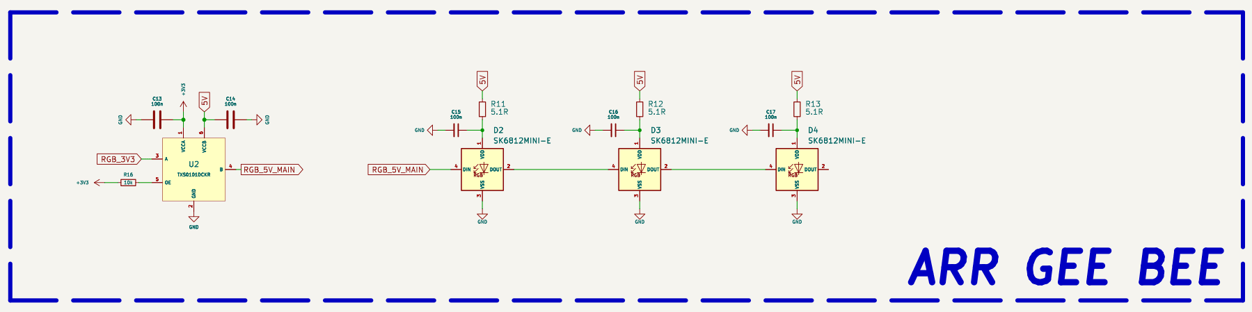
Praxis HE: level shifter (3.3 V → 5 V) and the three SK6812MINI-E LEDs in a chain.
Choosing an MCU
What MAGDA and the scanning scheme need:
| Requirement | Why | How to check |
|---|---|---|
| ADC-capable pins ≥ number of multiplexers, all on the same ADC peripheral | one ADC input per row, converted together in one sequence | count the channels of one ADC available on your package, not the family maximum; on parts with several ADCs, pins are split between them. The stock driver uses ADC1 |
| 12-bit ADC with multi-channel scan and DMA | all rows of a column in one conversion sequence | reference manual, ADC chapter |
| Full-speed USB | QMK connection | datasheet |
| An accurate USB clock | USB needs 48 MHz within tight tolerance | on STM32F4 this needs a crystal (HSE); Praxis uses 8 MHz |
| Enough RAM | QMK's wear-leveling keeps a RAM copy of the settings storage | a few KB beyond QMK's own needs |
| QMK/ChibiOS support | firmware platform | QMK's list of compatible microcontrollers |
| MAGDA driver support | the stock mux_adc driver |
initially STM32 families with the ADCv2 peripheral (F2, F4, F7); others need a driver port |
DMA streams. The sensor ADC, the SPI bus to the settings flash and the LED driver (a PWM timer, or SPI) each move data by DMA, and no two of them can share a DMA stream. On STM32F4 each peripheral can only use the specific streams listed in the reference manual's DMA request tables, so choose the ADC, SPI and timer (and with them the pins) together and check that their streams do not collide. Praxis uses ADC1 (DMA2 stream 4), SPI1 (DMA2 streams 0 and 3) and TIM1 for the LEDs (DMA2 stream 5).
Recommendation: STM32F401 or STM32F411 with an 8 MHz crystal. They meet every requirement above, the stock driver supports them, and QMK's generic board configurations for them expect an 8 MHz crystal, so no clock configuration is needed. Check that the ADC pins you need are free of other functions you also need; on Praxis, PA0–PA4 carry the five row signals and PA5–PA7 carry SPI to the flash.
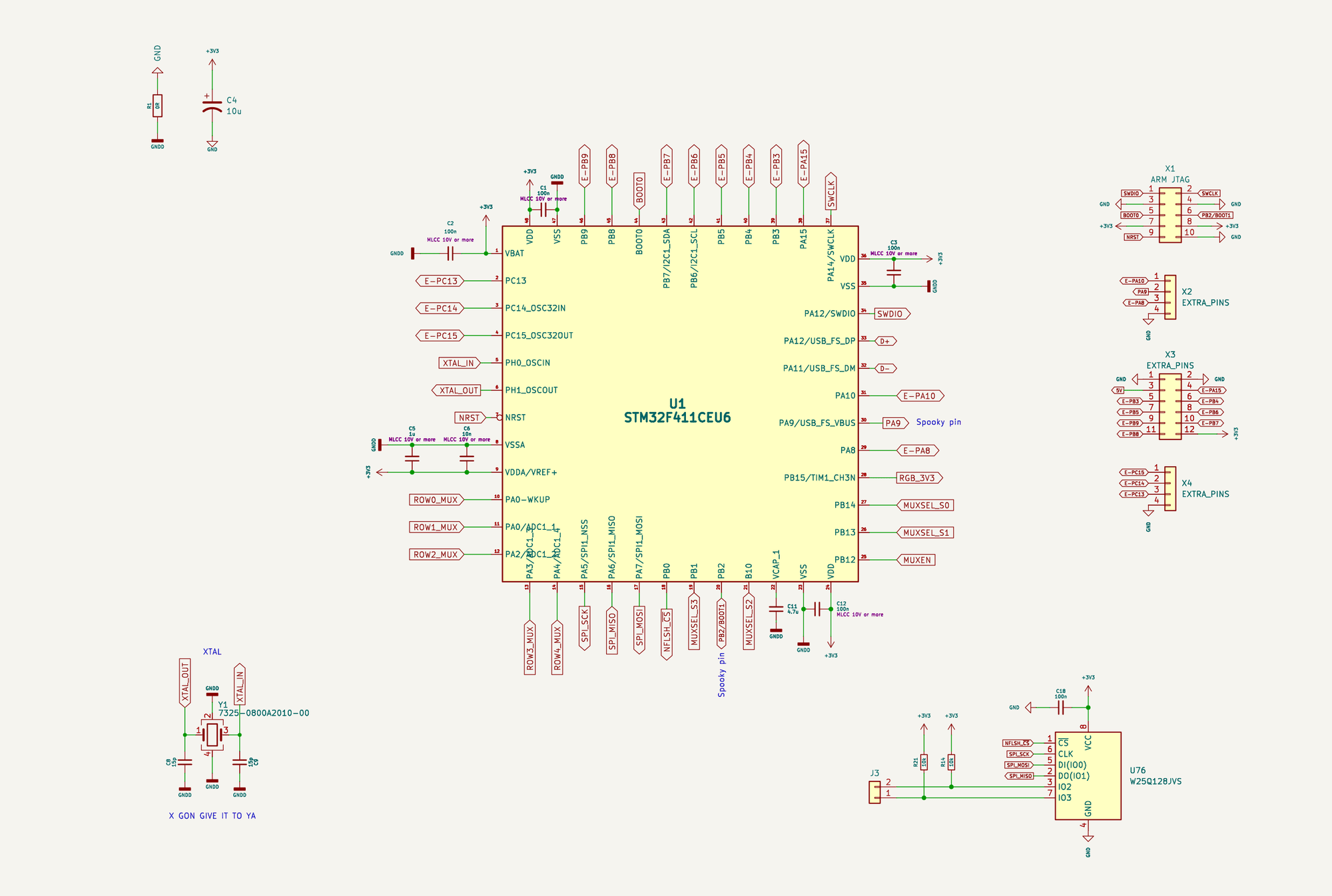
Praxis HE: STM32F411CEU6 with the row signals on PA0–PA4 (ADC1), the multiplexer select lines and enable on PB14, PB13, PB10, PB1 and PB12, the external flash on SPI1 (PA5–PA7, chip select PB0), the 8 MHz crystal and the SWD header.
Choosing a sensor
Use a linear Hall sensor with an analog, ratiometric output. Most Hall-effect sensors on the market are not of this kind: they are Hall switches (and latches), with a digital output at logic levels. The output goes high once the field crosses an operating threshold and back low once it falls below a release threshold, and the chip reports nothing in between. That is one fixed actuation point set by the part, with no travel to measure, so no adjustable actuation, calibration or rapid trigger. These sensors cannot be used; check that the datasheet describes an analog output proportional to the field (often called a linear Hall sensor). Magnetoresistive (TMR) sensors with an analog output also fit MAGDA's one assumption, a reading monotonic in travel; check their output range and supply behavior against the same criteria.
| Parameter | What to look for | Praxis example (HAL4904 at 3.3 V) |
|---|---|---|
| Supply range | includes 3.3 V, since the sensor shares the ADC reference rail | 2.5–6.5 V |
| Supply current | × number of keys must fit the USB budget (step 2) | 1.4 mA |
| Sensitivity | matched to the magnet (below) | 1.4 mV/G |
| Output range | rail to rail is best; note nonlinearity near the rails | 0 to VDD, slightly nonlinear at the edges |
| Zero-field output | at half the supply (bipolar), known and stable; MAGDA's travel curve uses it | VDD/2 (ratiometric) |
| Output noise | small compared with the ADC step | 1.4 mV RMS |
| Response time | microseconds or less, so it never limits scanning | about 1 µs |
| Output resistance | low, for fast settling through the multiplexer | 120 Ω |
| Package and polarity | small, placeable under the switch; know which face is sensitive and the polarity sense | SOT-23; sense reversed relative to its through-hole version |
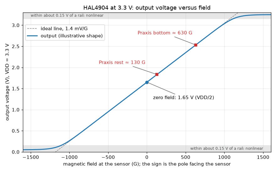
HAL4904 at 3.3 V: output voltage versus the field at the sensor. At zero field the output sits at 1.65 V, half the supply; it rises for one pole and falls for the other at 1.4 mV/G, linearly over most of the range, and bends only within about 0.15 V of either rail, where it flattens out. This plot is based on the HAL4904 datasheet's sensitivity and zero-field output; curves change between sensors, so check the datasheet of the sensor you choose. The red squares are the Praxis HE's key R0C7 at rest (about 130 G) and fully pressed (about 630 G), both well inside the linear part; the actual measurements for this key, readings with their voltage and field at every depth, are in the table under Result on the Praxis HE in step 11.
Zero field at half the supply. Ideally the sensor outputs half its supply with no field and swings both ways: up for one magnetic pole, down for the other (a bipolar sensor). There is no standard among the manufacturers of magnetic switches for computer keyboards, so some switches present a north pole to the sensor and others a south pole, with varying levels of strength. With a half-supply zero field, the same PCB works with both kinds: the reading moves up for one and down for the other, and MAGDA learns the direction of each key at calibration. Not every ratiometric linear sensor is like this: some put the zero-field output near one rail, or elsewhere off the middle, and swing mostly in one direction (unipolar sensors). A board built with one of them can only serve switches of one magnet orientation; with the other, the reading runs into the rail instead of following the key. Check the zero-field output (often called quiescent output voltage) in the datasheet.
The sensor to look for therefore combines both properties: a linear, ratiometric analog output and a zero field at half the supply.
Output inside the ADC range. The sensor's output must stay within what the ADC can read, 0 V to its reference (VREF+). The simplest way to guarantee this is the one Praxis HE uses: the sensors are fed from the same 3.3 V rail, made by the DC-DC converter, that feeds the MCU's VDDA/VREF+ (the PCB side is in step 2, Keep the measurement ratiometric). The sensor's output range is then automatically matched to the ADC's range: zero field reads mid-scale, and the full output swing maps onto the full ADC scale. If the sensor runs on a different voltage, or its output range does not match the ADC's, the signal has to be adapted before or after conversion:
- in the ADC, with internal gain or offset settings where the MCU offers them, which adds configuration and processing to the firmware;
- in analog hardware, with op-amp stages that shift and scale each signal into the ADC range, which adds parts, board area and cost, and new sources of offset and noise.
Both add complexity that a shared rail avoids.
Matching sensitivity to the magnet. The useful signal is the difference between the released and fully pressed readings, the span:
span in ADC steps ≈ (field at bottom-out − field at rest) × sensitivity ÷ ADC step
- Too little sensitivity gives a small span. Actuation points and rapid trigger then have coarse resolution and noise takes a larger share.
- Too much sensitivity saturates the output at the rail before full travel. The end of the key's travel is then lost.
Supporting a range of switches. Magnetic switches differ a lot in how strong a field they put on the sensor when fully pressed: some reach about ±400 G, others ±600 G, the strongest up to about ±1000 G. The sensitivity sets which of them a board can support:
-
Upper limit: the strongest field must still fit. With a 3.3 V supply and zero field at 1.65 V, the output can swing about ±1.5 V before it approaches the rails, where it turns nonlinear. The sensitivity must be at most that swing divided by the strongest field to support:
Strongest field to support Highest usable sensitivity HAL4904 (1.4 mV/G) at that field ±400 G 3.75 mV/G 560 mV, 695 counts ±600 G 2.50 mV/G 840 mV, 1043 counts ±1000 G 1.50 mV/G 1400 mV, 1738 counts To support ±1000 G switches, a board needs a sensor with a lower sensitivity than one designed only for ±400 G switches.
-
Lower limit: enough counts and a good signal-to-noise ratio. The span in counts grows with the sensitivity. A low sensitivity leaves few counts across the keystroke, so actuation points and rapid-trigger distances get coarse, and the board's own noise (fixed in millivolts, from the PCB and the ADC) becomes a larger share of the signal.
- Choose the highest sensitivity that still fits the strongest switch to support, with some margin. The HAL4904 at 1.4 mV/G supports up to about ±1000 G. The Praxis HE's switches reach about 630 G fully pressed (calibrated bottom 3135 counts on R0C7, rest about 130 G), using about 60 % of the available swing: room for stronger switches, at the cost of some resolution with the ones fitted.
Aim for the fully pressed reading to stay inside the sensor's linear output range, with the span covering a good part of it. The reading is not proportional to key travel: the field grows steeply as the magnet approaches, so most of the reading change happens in the last part of the keystroke. MAGDA corrects for this with a travel curve (step 3). The flip side is that the top of the keystroke is where readings change least, so sensor noise limits how high an actuation point can usefully be set; a larger span helps there. The field depends on the switch's magnet and its distance to the sensor: ask the switch manufacturer for the field at rest and at bottom-out, or measure a prototype with MAGDA's raw-value console output (step 6).
How much EEPROM, and why external SPI flash is recommended
An analog keyboard stores much more than an ordinary one: every key has its own calibration. QMK sizes its stored data from the matrix, so the total grows with the number of keys.
| Stored data | Praxis HE (75 matrix positions) | Full-size board (108 positions) |
|---|---|---|
| QMK's own settings | 37 bytes | 37 bytes |
| MAGDA calibration and global settings (today) | 304 bytes | 436 bytes |
| MAGDA per-key settings (planned, estimate) | about 0.7 KB | about 1 KB |
| VIA keymap (4 layers) | about 0.6 KB | about 0.9 KB |
| VIA macros | at least 0.5 KB to be useful | at least 0.5 KB |
| Total with everything | about 2.1 KB | about 2.8 KB |
Plan for 2–3 KB of emulated EEPROM, and set the firmware's EEPROM size to match (in QMK, logical_size for wear-leveling). QMK keeps a RAM copy of the whole emulated EEPROM, so this also costs the same amount of RAM. The full breakdown is in the MAGDA specification, section 4.2.
There are two places to put it:
Internal MCU flash. On STM32F401/F411, QMK's emulated EEPROM gives 1 KB of usable storage and uses a 16 KB flash sector. That 1 KB holds QMK's settings and MAGDA's calibration, but not per-key settings together with a VIA keymap. The storage also shares the MCU's flash with the firmware.
External SPI NOR flash. A small, inexpensive chip on one SPI bus plus a chip-select pin.
- QMK's wear-leveling spreads writes across it, so repeated saves do not wear it out.
- It offers several KB of usable storage. Praxis uses 4 KB, limited on purpose, because QMK keeps a RAM copy of that size.
- Flashing new firmware into the MCU never touches it, so calibration survives firmware updates. The data only becomes invalid if its format changes, and MAGDA detects that through a version tag.
- It costs one chip, one SPI bus and one GPIO.
For an analog keyboard, where calibration data is per key and valuable, the external flash is the recommended choice. A board without it still works on internal flash within the 1 KB limit.
Step 2: Design the PCB
Scanning scheme
A magnetic-switch keyboard has one analog signal per key, 66 on Praxis HE, but the MCU has only a few ADC inputs. The scanning scheme reads every sensor through a handful of ADC inputs by taking turns, one column at a time.
The sensor matrix. Each sensor gets a position in a grid of rows and columns, written RrCc: R0C0 is row 0, column 0; R2C7 is row 2, column 7. Unlike a switch matrix, the grid is only a way of organising the wiring: every sensor has its own output net named after its position, and no two sensors share a wire. The grid need not follow the physical rows of keys either: Praxis HE's layout is angled and split, and the table below maps each position to its key. Praxis HE uses 5 rows and 15 columns; 66 of the 75 positions have a sensor. The labels are the key legends from the schematic:
| C0 | C1 | C2 | C3 | C4 | C5 | C6 | C7 | C8 | C9 | C10 | C11 | C12 | C13 | C14 | |
|---|---|---|---|---|---|---|---|---|---|---|---|---|---|---|---|
| R0 | 6 | 5 | 4 | 3 | 2 | 1 | GRV | ESC | LBSPC | PLUS | MINUS | 0 | 9 | 8 | 7 |
| R1 | T | R | E | W | Q | TAB | PGUP | SLSH | RBRKT | LBRKT | P | O | I | U | Y |
| R2 | G | F | D | S | A | CAPS | PGDN | ENTER | RBSPC | QUOT | SCLN | L | K | J | H |
| R3 | · | B | V | C | X | Z | LSFT | SLSH | DOT | COMMA | M | N | B | RSFT | MO1 |
| R4 | · | · | · | MO1 | LSPC | LCTL | LALT | · | RSPC | · | RALT | · | · | · | RCTL |
· = no sensor: that multiplexer input is tied to ground.
Notice that the sensor matrix does not match how the keys are physically laid out: ESC, the top-left key, sits in R0C7, between GRV and the left Backspace. This is because the function of each key is set in firmware, so sensor positions can be chosen for convenience of wiring and other design constraints. QMK bridges the two with the board's LAYOUT macro, defined in keyboard.json: each physical key is listed with its position on the board and the matrix position it is wired to (on Praxis, {"label": "ESC", "matrix": [0, 7], "x": 0.432, "y": 0}), and keymaps then list keycodes in physical order.
Even so, on the schematic each sensor carries a label with its key's legend (the ESC, GRV, TAB… in the figure below, and the labels in the table above). They serve organisation and bookkeeping, and make each sensor easy to identify when working on a live prototype.
The full sensor matrix from the schematic. Each column of the drawing is one matrix column, C0 at the left to C14 at the right, with rows 0 to 4 from top to bottom (open the image at full size to read the labels):

Praxis HE: 66 HAL4904 sensors, all powered from +3V3, each output on its own net (R0C0, R1C0, …). Positions with no key (R3C0, R4C0, R4C1, R4C2, R4C7, R4C9, R4C11, R4C12, R4C13) are tied to ground.
One multiplexer per row. Each row's sensor outputs go into an analog multiplexer. A multiplexer is an electrically controlled selector switch: it has many inputs, one output (its common pin), and a few select lines that choose which input is connected to the output. The CD74HC4067 has 16 inputs and 4 select lines; the binary number on the select lines is the input it connects. Praxis HE wires input c of the multiplexer for row r to sensor RrCc, so the multiplexer's input number is the column number. Each multiplexer's output goes to its own ADC input on the MCU: row 0 to PA0, row 1 to PA1, and so on up to row 4 on PA4.
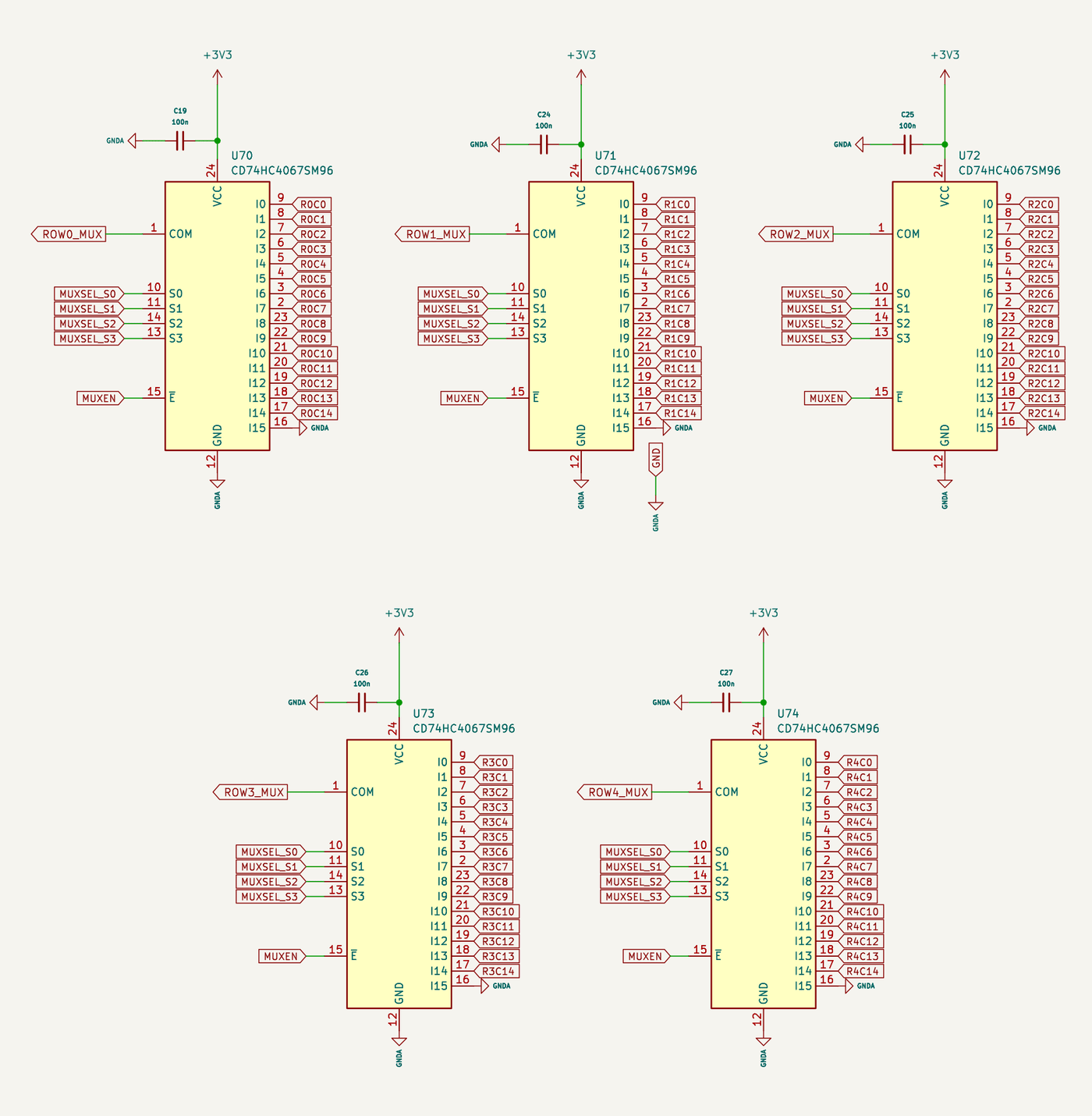
Praxis HE: the five CD74HC4067 multiplexers, U70 to U74 for rows 0 to 4. Inputs I0–I14 take the row's sensors, columns 0 to 14; input I15 is grounded. All five share the select lines MUXSEL_S0–S3 and the enable MUXEN; each common pin (ROW0_MUX to ROW4_MUX) goes to its own ADC input.
Sweeping the columns. All five multiplexers share the same select lines, so they always select the same input number, that is, the same column. That is what makes the scan work:
- The MCU puts column 0 on the select lines (binary 0000). Every multiplexer now connects its input 0: multiplexer 0 shows R0C0 at its output, multiplexer 1 shows R1C0, multiplexer 2 shows R2C0, and so on.
- It waits a few microseconds for the outputs to settle to the new sensors' voltages (see Scan timing).
- The ADC converts its five inputs, PA0 to PA4, one after the other in a single sequence. The results are the readings of R0C0, R1C0, R2C0, R3C0 and R4C0: the whole of column 0.
- The MCU then selects column 1 (binary 0001). Every multiplexer switches to input 1, and the same conversion now reads R0C1 to R4C1.
- It carries on through column 14 (binary 1110).
After the last column, every sensor has been read once: that is one full scan of the matrix, a frame, and the scan starts again from column 0. Praxis HE therefore needs 15 select steps per frame, each reading 5 sensors at once:
| Select step | Select lines S3–S0 | Mux 0 → PA0 | Mux 1 → PA1 | Mux 2 → PA2 | Mux 3 → PA3 | Mux 4 → PA4 |
|---|---|---|---|---|---|---|
| 0 | 0000 | R0C0 | R1C0 | R2C0 | R3C0 | R4C0 |
| 1 | 0001 | R0C1 | R1C1 | R2C1 | R3C1 | R4C1 |
| 2 | 0010 | R0C2 | R1C2 | R2C2 | R3C2 | R4C2 |
| … | … | … | … | … | … | … |
| 14 | 1110 | R0C14 | R1C14 | R2C14 | R3C14 | R4C14 |
One way to picture it: the sensor matrix is a spreadsheet, the multiplexers are five readers, one per row, and the select lines point all of them at the same column. The MCU moves the pointer one column at a time and writes down the five values each time.
The arrangement sets the board's limits. The number of rows is the number of multiplexers and ADC inputs; the number of columns is limited by the multiplexer's inputs (16 for the CD74HC4067, one of which Praxis keeps grounded). The scan time grows with the number of columns (select steps), not with the number of keys, because each step reads all rows at once.
Multiplexer inputs with no key, and any spare input of every multiplexer (I15 on Praxis), are tied to ground: they read 0 V, which bring-up uses to check the multiplexer and ADC path.
Keep the measurement ratiometric
This is the PCB side of the sensor choice in step 1 (Output inside the ADC range). A ratiometric sensor's output is a fixed fraction of its supply for a given field: its zero-field output and its sensitivity both scale with the supply. Feeding the sensors from the same rail as the ADC reference gives two things at once:
- Matched ranges. The sensor's output range is the ADC's input range, with no gain or offset stage in between (step 1).
- Supply changes cancel. A 1 % drop in the rail lowers both the sensor output and the ADC full scale by 1 %, and the reading is unchanged. This covers slow changes of the rail, with load or temperature; it does not cancel ripple, which is a noise problem (Noise).
Recommendation: power the sensors from the rail that feeds VDDA/VREF+
This is a rule of thumb, not a requirement. Sensors on a separate regulator, or an ADC reference independent of the sensor supply, can still work: the signal can be adapted in the ADC or with op-amp stages (step 1), and the supply drift that no longer cancels has to be kept small or corrected. A shared rail is the best case because it needs neither: the firmware reads raw counts directly, and the hardware has no extra parts. Praxis HE follows it.
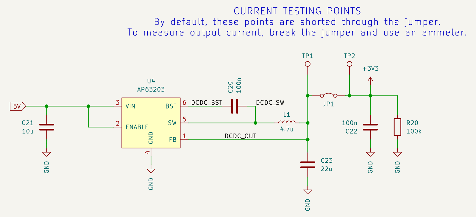
Praxis HE: the AP63203 buck converter makes the single 3.3 V rail that feeds the sensors, the multiplexers and the MCU's VDDA/VREF+. JP1 and TP1/TP2 allow measuring the board's current.
Current budget
Sensors are always powered in a simple design, so their current adds up: total sensor current ≈ number of keys × sensor supply current. For Praxis: 66 × 1.4 mA ≈ 92 mA at 3.3 V.
- USB limit. A standard USB 2.0 port provides 500 mA. Check the total, including LEDs and MCU, against that.
- Suspend current. USB suspend allows only 2.5 mA, which no always-on sensor array meets. Most hosts do not enforce it. Meeting it would need a switch that cuts sensor power during suspend, which Praxis does not have.
- Voltage drop. Long, thin supply traces make the local supply at each sensor slightly different. Per-key calibration absorbs this static difference, but wide traces or a plane keep it small.
Power supply: a DC-DC converter rather than an LDO
Ordinary keyboards make their 3.3 V with a linear regulator (LDO): the MCU draws a few tens of milliamperes, so the LDO stays cool, and it is simple and quiet. A magnetic-switch keyboard adds an always-on sensor array that draws several times more, and at that current the LDO's inefficiency starts to matter. The Praxis HE therefore uses a synchronous buck converter (AP63203) from USB's 5 V.
An estimate for the Praxis load: about 92 mA of sensors plus roughly 30 mA for the MCU (an assumption), about 120 mA at 3.3 V (0.40 W):
| LDO | Buck converter (≈ 90 % efficient, typical) | |
|---|---|---|
| Power lost as heat | (5 − 3.3) V × 0.12 A ≈ 0.21 W | ≈ 0.04 W |
| Efficiency | 3.3 ÷ 5 ≈ 66 % | ≈ 90 % |
| Current drawn from USB | ≈ 122 mA (the load current itself) | ≈ 89 mA |
- Heat is the main reason. An LDO turns the voltage difference into heat on the board, about 0.2 W here: in a small package (for example SOT-223, roughly 60 °C/W) that is a local rise of around 12 °C, spreading into the PCB under the keys. Temperature changes move both the sensors' output and the magnets' field (sintered NdFeB magnets lose on the order of 0.1 % of their field per °C), so a warming board shifts rest levels and calibration. A buck converter keeps that heat about five times smaller.
- USB current. A linear regulator draws the full load current from USB; a buck converter draws less than the load, which leaves more of the budget for LEDs and anything else on 5 V.
- The first drawback of DC-DC converters is noise. A buck converter switches its output at a high frequency, and that ripple can reach the sensors and the ADC reference, which is exactly what the noise warning below is about. Choose a converter with a high switching frequency and good light-load behaviour. Ratiometric measurement cancels slow supply changes, not ripple.
- The second drawback is switched-converter PCB design requirements. An LDO is a linear device that is not switched, so it introduces no problematic design constraints and is forgiving in implementation; a buck converter is not. Its board layout decides how much of that switching noise reaches the analog signals:
- Tight current loop. The input capacitor, the converter's input and ground pins and the switch carry fast, pulsed currents. Place the input capacitor right at the pins and keep that loop as short and wide as possible; the loop area is what radiates.
- Small switch node. The node between the converter and the inductor swings between 0 V and the input voltage at every cycle, with sharp edges. Keep its copper just big enough for the current, and route nothing sensitive next to it or under the inductor. A shielded inductor helps.
- Well grounded. Give the converter a solid, unbroken ground plane with vias close to its ground pins, so its return currents stay local and do not flow under the analog section.
- Well away from the analog signals. Place the converter far from the sensors, the multiplexers and the traces that carry their outputs to the ADC, for example near the USB connector at the board's edge. Long multiplexer-to-ADC traces are the most exposed (190–240 mm on Praxis).
- Well-filtered voltages. Low-ESR ceramic output capacitors as the datasheet specifies, a ferrite bead or RC between the 3.3 V rail and VDDA, and local decoupling at every multiplexer and sensor.
- Quiet feedback. Keep the feedback trace short and away from the switch node and the inductor.
- Start from the datasheet. Converter datasheets include a recommended layout; follow it closely.
- The third drawback is cost: converters are cheap themselves but cost more in ancillary components and make the bill of materials larger. Besides the converter, a buck needs an inductor, input and output capacitors, a bootstrap capacitor and often a feedback divider, plus the VDDA filter, where an LDO needs little more than two capacitors. More parts also mean more board area and more placements at assembly.
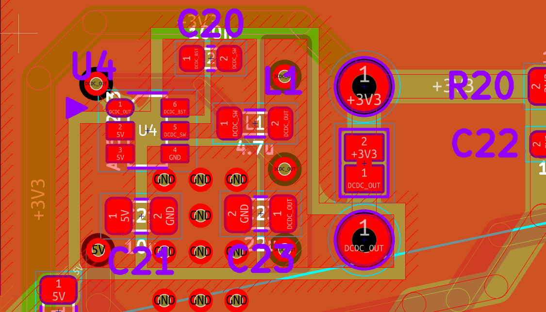
Praxis HE: the buck converter's layout, and how it follows the second drawback's requirements:
- Tight current loop: the input capacitor C21 (10 µF, 5V to GND) sits directly below U4 (AP63203), next to its input and ground pins, so the pulsed input current flows round a very small loop.
- Small switch node: DCDC_SW is a short copper patch from U4's switch pin to the inductor L1 (4.7 µH) right beside it, shared only with the bootstrap capacitor C20 (100 nF, DCDC_BST to DCDC_SW) above the chip.
- Well grounded: the ground pads of U4, C21 and the output capacitor C23 (22 µF, DCDC_OUT to GND) land on one ground area, stitched by a row of vias to the two inner copper layers, which are ground on this four-layer board.
- Well away from the analog signals: the converter is grouped compactly in its own area of the board, far apart from the sensing chain, on the same ground as the rest of the board.
- Quiet feedback: U4's feedback pin (pin 1, DCDC_OUT) connects through a via right at the pin, on the opposite side of the chip from the switch pin and the inductor.
- Well-filtered voltages and measurement: C23 filters the converter's output. The solder jumper JP1 joins DCDC_OUT to the +3V3 rail, with through-hole test pads on either side, TP1 on DCDC_OUT and TP2 on +3V3 (see the recommendation below); C22 (100 nF) decouples +3V3 after the jumper, and R20 (100 kΩ, +3V3 to ground) gracefully discharges the bulk capacitors when the board is unplugged.
Recommendation: add a jumper with through-hole probes so that one can open the jumper to measure current with an ammeter
Put the jumper in series with the 3.3 V output, with a through-hole test point on each side. Opening the jumper and connecting an ammeter across the two points gives the board's real current instead of an estimate. Praxis HE has this: JP1 is a solder jumper, bridged by default, that is cut open for the measurement and re-soldered afterwards; TP1 and TP2 are through-hole test pads (2 mm pad, 1 mm drill) on either side.
The sensors set the power budget. Whatever the regulator, linear Hall sensors are current-hungry: each draws about 1.4 mA (HAL4904), continuously, so the sensors alone take 92 mA on the Praxis HE and about 146 mA on a 104-key board. That leaves correspondingly less of USB's 500 mA for RGB lighting (addressable LEDs draw tens of milliamperes each at full white), and it rules out long battery life: a 2000 mAh battery would run the Praxis HE's sensors alone for under a day (about 22 h).
For power efficiency, use TMR sensors. They are resistive bridges with a high resistance, so they draw microamperes rather than milliamperes: at, for example, 10 µA per sensor (an illustrative figure; check your part's datasheet), 66 sensors draw about 0.7 mA, over a hundred times less, which frees the USB budget for lighting and makes wireless designs practical. MAGDA's one assumption (one reading per key, monotonic in travel) covers TMR sensors; a TMR sensor beside the magnet rather than under it needs its own travel curve (MAGDA architecture, section 3.2; step 3 and step 11).
Noise
Noise is the most stringent quantity of the whole design
Noise decides how small everything else can be: the lowest usable actuation point, the gap between press and release, the smallest rapid-trigger distance, and the calibration noise bound. Magnets and linear Hall sensors are very stable, so in a magnetic-switch keyboard most of the noise comes from the PCB design itself: the supply and its ripple, grounding and return paths, routing next to switching or data lines, and the analog path to the ADC. Design the board for low noise from the start; firmware can only filter it, at the cost of response time.
On the Praxis HE, idle noise measured about 3× the sensor's datasheet figure (5.8 against 1.7 counts RMS), while the grounded multiplexer inputs stayed quiet (0–2 counts). The excess therefore entered on the sensor side of the multiplexers, its supply and wiring, not in the multiplexers or the ADC (an inference from those measurements; step 7).
The key position is read from millivolt-level changes, so noise sets the useful resolution.
- Know the numbers. Compare the sensor's output noise with the ADC step. For Praxis, 1.4 mV RMS against 0.81 mV per step is about 1.7 steps RMS on paper; the measured noise was about 3× that (step 7). A noisier sensor or a lower-resolution ADC leaves less room for low actuation points and small rapid-trigger distances.
- Decoupling. Place a 100 nF capacitor at each multiplexer and at each MCU supply pin, and decouple VDDA separately and close to its pin. Consider local decoupling for groups of sensors.
- Filtering VDDA. A ferrite bead or small RC between the 3.3 V rail and VDDA keeps switching-regulator ripple out of the ADC reference. Ratiometric operation cancels slow drift, not ripple.
- Routing. Keep the multiplexer outputs, which are the analog lines to the ADC, away from the regulator's switching node, the LED data line and the USB pair. Give every analog trace a continuous ground plane on the adjacent layer.
- Ground pours under switches. See the keep-out zone under Sensor placement.
Scan timing
scan time ≈ number of select steps × (settling time + conversion time for all rows)
- Settling. After the select lines change, the multiplexer output must settle before sampling, set by the sensor's output resistance plus the multiplexer's on-resistance charging the trace and ADC input capacitance. With a 120 Ω sensor and a 4067 at 3.3 V, the time constant is tens of nanoseconds, so about 1 µs of settling is ample.
- Conversion. At 12 bits, converting one ADC channel on an STM32F4 takes on the order of a microsecond, depending on the ADC clock and sample time.
- In practice the firmware loop adds overhead: Praxis runs about 2000 scans per second (step 7), comfortably faster than USB's 1 ms polling.
Long analog traces add capacitance and settling time. Placing the multiplexers close to the MCU keeps the analog runs short.
Wiring rules for the stock driver
MAGDA's stock mux_adc driver works without custom code if the board follows these rules:
- One multiplexer per matrix row, its common pin on its own ADC-capable MCU pin.
- All those pins are channels of the same ADC peripheral: one select step converts all rows as a single sequence on one ADC. Check each pin's ADC in the datasheet's pin table. The stock driver currently uses ADC1; a board whose rows are all on another ADC needs a driver change or its own backend.
- All multiplexers share the same select lines, least significant bit first, and optionally one shared enable.
- Multiplexer input k is matrix column k. The driver assumes this identity mapping; scrambled wiring needs a custom backend.
- Unused inputs tied to ground.
A board that breaks these rules can still use MAGDA, by writing its own backend (driver documentation).
Sensor placement
- Position. Center each sensor exactly where the switch's magnet sits, following the switch manufacturer's footprint.
- Orientation. Keep the same orientation for every sensor. The sensor's sensitive point may not be exactly at the package center, so a rotated sensor sees a slightly different field. Calibration absorbs this, but consistent placement keeps keys alike.
- Stabilizers. Keep the orientation consistent under stabilized keys as well.
Keep-out zone around each sensor
A Hall sensor measures whatever magnetic field reaches it, not only the switch magnet's, and it sits on the same board as noisy digital circuits. On Praxis HE, each sensor is protected by a keep-out zone 14 × 14 mm wide. The zone is part of the switch footprint and, as the board enforces it, only forbids copper pour on all four copper layers; tracks, vias and pads may still pass. Everything else in the list below is design discipline that the footprint does not check. The sensor's own supply decoupling, if fitted, belongs inside the zone, placed close to the sensor. While electromagnetic coupling is a notably difficult subject, here is a discussion of what to keep out and why:
- Copper pour. Praxis leaves the zone free of pour on all layers, as many magnetic-switch footprints ask. Copper itself does not change a static magnetic field; the reason is what pours carry: return currents of other circuits, and coupling from nearby noisy nets, right at the sensor. Keeping every sensor's surroundings identical also keeps keys alike. On a four-layer board, weigh this against keeping the inner ground planes solid.
- Magnetic materials. Ferrite-cored inductors and beads, steel screws, standoffs and brackets, and parts with nickel-plated terminations bend and concentrate the magnet's field. Near a sensor, they change that key's rest and bottom readings and the shape of its travel curve, so the key behaves unlike its neighbours and a factory calibration no longer fits. A magnetised part adds a constant offset of its own.
- Current-carrying traces. A current makes its own magnetic field: by the straight-wire estimate, about 0.2 G at 1 mm from a trace carrying 100 mA, only a fraction of a count on the HAL4904. Changing currents are the concern: LED PWM, the DC-DC converter's loops, loads switched on and off. They move the reading in step with the load, and a large enough current does so by whole counts. Route power and high-current traces away from the sensors, never underneath them.
- Fast digital signals. Clock, SPI and LED data lines and the multiplexer select lines have sharp edges that couple capacitively into the sensor's output and supply, adding noise the filter can only partly remove. Keep them out of the zone, and cross the sensor's output trace at right angles where they must cross.
- Anything in the switch's way. The sensor sits where the magnet's field is strongest and most repeatable, usually centred under the stem; nothing may push it off that spot or obstruct the switch (pins, stabilizer wires, tall parts).
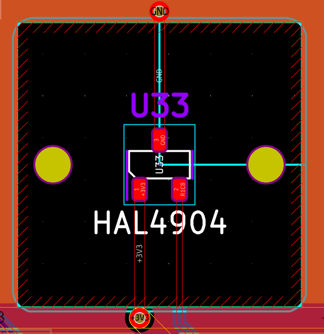
Praxis HE: sensor U33 (R1C8) in its 14 × 14 mm keep-out zone, the hatched square. The copper pour stops at the zone's edge; inside there is only the sensor and its three traces, +3V3, GND and its output R1C8. The supply and ground traces leave the zone to vias just outside it. The two round pads on either side belong to the switch footprint.
What is true and what is not on copper around sensors
Not true: copper changes or blocks the magnet's field. Copper is not magnetic (it is very weakly diamagnetic, about a hundred-thousandth away from vacuum), so a pour does not change the shape or strength of a static field; a magnet held still over a pour reads the same as without it.
Not true: a ground pour acts as a Faraday cage and blocks the measurement. A Faraday cage keeps out electric fields and radio-frequency waves, not static magnetic fields. A conductor only screens a changing magnetic field once it is as thick as the skin depth, which in copper is about 2 mm at 1 kHz and about 20 mm at 10 Hz. A keystroke changes the field over milliseconds or longer, and a pour is 35–70 µm thick, tens to hundreds of times thinner: at these speeds it is transparent. Even a closed copper box would not stop the reading; blocking a static magnetic field takes a high-permeability material such as mu-metal or steel (see Magnetic materials above).
Not true, in practice: eddy currents in the pour disturb the reading. A moving magnet does induce currents in copper, but at keystroke speeds in a pour this thin they and their field are negligible, and they vanish when the key stops, so they cannot shift rest or bottom readings.
True: what a pour carries matters. A pour can carry the return currents of other circuits past the sensor, and couple noise from nearby nets into the sensor's output and supply. That is the reason for keeping it out of the zone, together with keeping every sensor's surroundings identical and following the footprint's own keep-out.
True: magnetic material does matter. Ferrite, steel and nickel bend and concentrate the field, and thick enough steel shields it.
If a board with ground pour under its sensors reads badly, look first for ferromagnetic material nearby (nickel-plated parts, a steel plate, steel screws), a sensor fitted with the wrong sensitive face or polarity, or noise coupled through the pour.
As a rule of thumb: use keep-out zones around sensors to avoid noisy signals, problematic couplings and pathologies in operation such as unreliable calibration and constant chattering. However, you might get away with placing some traces or regions somewhat close to the sensor; but there is no preemptive way to know in the design phase whether this will affect the readings, and finding out might cost you a prototyping round, so be careful and pedantic.
Getting into the bootloader
Warning
PROVIDE A HARDWARE WAY INTO THE BOOTLOADER
Flashing needs the MCU's bootloader. An analog keyboard cannot rely on holding a key at power-up, because keys may not register before calibration. Provide a hardware way in: a reset button plus BOOT0 access. Praxis uses a single button that resets on a tap and enters the bootloader on a hold. Minimally, expose the reset and boot pins for direct-pin operation.
Without a hardware way in, it will be impossible to flash the microcontroller the first time, and the PCB will be unusable: a blank MCU has no firmware to jump to the bootloader from, and the only remaining route is a debug probe on the SWD pins, if they are exposed. Even after a first flash, the only route into the bootloader is through the firmware itself: a QK_BOOT key, or a key held at power-up. It is common for firmwares not to include QK_BOOT, and any firmware that fails to reach that point locks the board out. A build that crashes or hangs at start-up, a keymap without QK_BOOT, or a calibration that leaves no key registering are enough. The board can then only be recovered by opening it and bridging the MCU's pins by hand, or by soldering wires to them or to the SWD pads if they are reachable; on a finished keyboard this can mean desoldering switches, and at worst the board is bricked.
IN SHORT: PROVIDE A HARDWARE WAY INTO THE BOOTLOADER.
Step 3: Choose the travel curve
The field a sensor sees is strongly nonlinear in the magnet's distance: the reading barely moves at the top of the keystroke and changes fast near the bottom. Without correction, "10 % of the reading" is not 10 % of the keypress; on Praxis, with no correction, 10 % actuated around mid-travel and 90 % needed an almost full press. A travel curve converts readings to physical travel.
The right curve follows from the sensor type and its placement relative to the magnet, so decide it together with the parts and the PCB:
| Sensor and placement | MAG_TRAVEL_CURVE |
|---|---|
| Linear Hall sensor on the magnet's axis (under the switch, as on Praxis) | MAG_CURVE_POWER (default) |
| No model applies, or for comparison | MAG_CURVE_LINEAR (percent of the reading) |
| Other sensor types or geometries (e.g. a TMR sensor beside the magnet) | a new curve; how to add one: specification, section 3.2 |
For MAG_CURVE_POWER:
MAG_ZERO_FIELDis the sensor's output with no field, in raw counts: VDD/2 for a ratiometric sensor on the ADC reference rail, which is the default (2048). Take it from the datasheet otherwise; an error bends the curve most for keys whose rest reading is close to it.MAG_FIELD_EXPONENTstarts at the library default 3 (an ideal dipole) and is measured in step 11 (the Praxis HE measured n = 1).- A key whose rest reading is within 16 counts of
MAG_ZERO_FIELDdoes not fit the model and uses linear travel instead. On Praxis, one key (R0C1) does.
The noise margins tuned in step 10 are computed through the curve, so changing the curve later means repeating step 10.
Step 4: Create the keyboard directory
Add the MAGDA module repository to the QMK tree as modules/acheron, then write the port: keyboard.json (the acheron/mag module, matrix, layout, custom matrix, console, debounce 0, EEPROM), post_rules.mk (the backend, MAG_DRIVER), config.h (backend pins, a generous starting timing, the curve), halconf.h / mcuconf.h, the board's .c file (key mask, optional indicator hooks) and a default keymap. How, with every file's content: driver documentation.
Put these on a layer of the default keymap: QK_BOOT, MAG_CAL, MAG_DUMP, MAG_CAL_DUMP and EE_CLR. Keep EE_CLR away from keys you will press often on the same layer: on Praxis it first sat next to MAG_ACT_UP, accidental presses erased the calibration, and the result was first mistaken for sensor noise.
Make the timing values #ifndef-guarded in config.h, so step 7 can override them per build.
Pass: the firmware builds.
Step 5: USB and bootloader
Bring the board up before any sensing: leave out MAG_DRIVER and give the board a dummy backend, mag_hw_init doing nothing and mag_hw_scan filling every position with the same value (e.g. 2048). No key ever registers with a constant frame.
- Flash through the hardware bootloader entry (the reset button);
QK_BOOTis not reachable yet. - Check enumeration (
lsusbshows your VID/PID), reflashing, and any indicator driven by the host (e.g. Caps Lock). - Keep QMK's default EEPROM driver until step 9 if the external flash is not ready.
Pass: the board enumerates, reflashes, and its indicators respond.
Step 6: Raw scan
Enable the real backend (MAG_DRIVER = mux_adc) and stream readings with MAG_DUMP: every 100 ms, one raw and one trv line per row, then a blank line:
raw 0: 2231 2054 2181 ...
trv 0:    0    0    0 ...
raw covers every position, including unfitted ones; trv shows unfitted positions as -. Before calibration no key may register reliably, so the MAG_DUMP key can be hard to reach: turn streaming on from the board's code for this step (Praxis set the library's mag_dump_enabled flag after mag_init()), and remove that again afterwards.
Check:
- grounded inputs read about 0 (Praxis: 0–2 counts);
- idle sensors read a plausible rest level (Praxis: 2036–2376, above the 2048 zero-field level because of the magnet's bias at rest);
- pressing a key changes exactly one position, by a large amount (Praxis: about +900 counts for a full press).
Pass: all three hold for every key.
Step 7: Timing and noise
Timing sweep. Build the firmware with different MAG_SETTLE_US and MAG_ADC_SAMPLE_TIME values, e.g.
make <keyboard>:default EXTRAFLAGS="-DMAG_SETTLE_US=0 -DMAG_ADC_SAMPLE_TIME=ADC_SAMPLE_15"
At the fastest point, hold a key fully in column c and watch column c + 1 of the same row in MAG_DUMP (also the last column into the first, for the scan's wrap-around). If the next column moves out of its idle band, the multiplexer output has not settled: that point fails. Choose the smallest values with no carryover, then add margin. Praxis swept 0/1/2/5 µs × ADC_SAMPLE_15/28/56, saw no carryover even at the fastest point, and chose 2 µs / ADC_SAMPLE_28, two steps of margin on both.
Scan rate. Add #define DEBUG_MATRIX_SCAN_RATE to config.h for a test build: the console prints matrix scan frequency: N every second. Praxis runs about 1900–2000 scans per second. Rest drift (step 10) is set in scans, so note this figure. Readings vary with console and key activity.
Idle noise. With the chosen timing and nobody touching the keyboard, record MAG_DUMP for a few seconds (Praxis: 38 frames) and compute, for every key, the peak-to-peak spread of its raw reading. Praxis: median 26, 90th percentile 32, max 46 counts, about 3× the datasheet estimate. Grounded inputs share the multiplexer and ADC path; if they stay quiet while sensors are noisy, the noise comes from the sensor side.
The idle noise sets MAG_CAL_NOISE_BOUND (the maximum variation while calibration averages a rest level; default 64, twice the Praxis 90th percentile): if your 90th percentile is higher, raise it in config.h, or calibration keeps restarting keys. It is also the input for step 10.
Pass: no carryover at the chosen timing; noise measured.
Step 8: Calibration
Run the calibration (MAG_CAL), following the console messages; the user-facing procedure is the Calibration guide. Press each key once, one key at a time, and equally firmly: calibration records each key's deepest reading as its bottom, so a key pressed lightly gets a shallower bottom than one pressed hard, and the keys then actuate at noticeably different depths. Then press MAG_CAL_DUMP and look at the spans (bottom − rest):
- every key must have a rest and a bottom, and every key should move in the same direction (Praxis: all rising);
- spans should be similar; a key far below its neighbours was probably not pressed fully (long keys: press in the centre) and needs another calibration. Praxis: median about 790–850 counts depending on how firmly keys were pressed, minimum above 550;
- a key whose rest is close to
MAG_ZERO_FIELDuses linear travel (step 3).
Pass: every key calibrated, spans plausible, typing works.
Step 9: Persistence
Move to the final EEPROM backing if not done yet. Then check:
- calibration survives unplugging and replugging;
- calibration survives reflashing the firmware;
EE_CLRdiscards it (keys return to the factory table if the board has one, else to provisional behaviour).
MAG_CAL_DUMP shows each key's source: (stored) after calibrating; after EE_CLR, (factory) or provisional.
Pass: all three.
Step 10: Noise-margin tests and tuning
Why this is empirical
A key registers when its travel crosses the actuation point and releases below a slightly higher point (the hysteresis). Near the top of the keystroke the reading changes very little per unit of travel, so at low actuation levels these points are only a few raw counts apart, comparable to the sensor noise. How many counts depends on each key's rest field, the magnet, the noise and the scan rate. The model below predicts the margins, but only testing with a hand on the keys shows whether a setting works, and some effects (such as how fast rest drift follows a finger) are not in the model at all.
The loop: calibrate → compute the margins from MAG_CAL_DUMP → run the tests → change one parameter → retest.
Computing the margins
The margins are computed through the travel curve, so they rest on the curve's model. MAG_CURVE_POWER takes the field of the switch magnet in its asymptotic, large-distance form, a single power of the magnet-to-sensor distance \(z\) (Background: the magnetic dipole, step 11):
where \(x\) is a raw reading, \(B_0\) the reading at zero field and \(C\) a constant for the key (magnet strength, sensor gain, ADC scale). The position \(p(x)\) below is this distance without the constant \(C^{1/n}\), which cancels when travel is scaled between the key's rest and bottom.
For MAG_CURVE_POWER, with \(B_0\) = MAG_ZERO_FIELD, \(n\) = MAG_FIELD_EXPONENT and a key's rest and bottom from MAG_CAL_DUMP:
-
the position of a reading \(x\), and its values at the key's rest and bottom:
\[ p(x) = \dfrac{1}{\lvert x - B_0 \rvert^{1/n}}, \qquad p_r = p(\mathtt{rest}), \qquad p_b = p(\mathtt{bottom}) \]\(p_r\) is the position with the key at rest, not pressed; \(p_b\) is the position with the key fully pressed, at the bottom of its travel.
-
the travel \(t\) (from 0 to 1) of a reading \(x\):
\[ t = \dfrac{p(x) - p_r}{p_b - p_r} \] -
the reading at travel \(t\):
\[ \lvert x - B_0 \rvert = \dfrac{1}{\left[\, p_r + t\,(p_b - p_r) \,\right]^{n}} \]
These formulas are only as accurate as that approximation. For the Praxis HE, the depth sweep of step 11 (Result on the Praxis HE) confirms it with a fitted exponent: with \(n = 1\) the curve places a reading within 0.08 mm rms of the key's measured depth, while the dipole's own \(n = 3\) is off by 0.35 mm rms and actuates up to about 0.4 mm deeper than set. Compute the margins with the exponent the board ships with, fitted in step 11 where possible, not with the dipole's 3: a different exponent moves where each percentage sits in raw counts, and so changes every gap. The fit covers one sweep of one key, with the zero field assumed, not measured; margins on keys resting close to \(B_0\) are the most sensitive to both.
Travel units are fractions of 1023. For each key, compute the reading at the actuation point and at the release point (actuation − MAG_HYSTERESIS_DEFAULT); their difference in raw counts is the key's gap. Compare the smallest gaps with the filtered noise: the filter (MAG_FILTER_SHIFT 2) cuts idle peak-to-peak noise to roughly \(0.4\times\) (Praxis: about 10–13 counts). Keys whose rest is closest to \(B_0\) have the smallest margins; test those.
Praxis example (\(n = 3.5\), one calibration, computed before the exponent fit of step 11): at 20 % actuation with a hysteresis of 32 travel units, gaps were 6–11 counts; with 64, 10–21. With the fitted \(n = 1\) the low levels sit closer to rest in raw counts and their gaps shrink (at 10 %: 3–11 counts, against 7–17 with \(n = 3\)), so repeat the tests at low levels after changing the exponent.
Parameters, in order of importance
Defaults are listed in the specification, section 3.4; override them in the board's config.h.
| Parameter | Raising it | Lowering it |
|---|---|---|
MAG_HYSTERESIS_DEFAULT |
removes chatter at low levels; the key must rise further to release (and rapid trigger resets later) | releases sooner; chatter when the gap is below the noise |
MAG_DRIFT_SHIFT |
rest follows only slow changes (a resting or slowly moving finger no longer shifts it); real drift (e.g. temperature) is followed more slowly | rest follows faster; a slow press or a resting finger drags the actuation point away |
MAG_FILTER_SHIFT |
less noise, more latency (time constant about 2^shift scans) | faster response, more noise |
MAG_REST_WINDOW |
drift and the held-at-power-up check accept larger offsets | drift stops for smaller offsets |
MAG_ZERO_FIELD, MAG_FIELD_EXPONENT |
shape of the curve (step 3, step 11) | |
MAG_SETTLE_US, MAG_ADC_SAMPLE_TIME |
the noise floor itself (step 7) |
Drift runs every scan, so its time constant is 2^MAG_DRIFT_SHIFT scans: with the default 16 and about 2000 scans per second, about 33 s.
The tests
Run them at the lowest actuation level the board offers (10 %) and a few levels above, on the keys with the smallest margins. Watch key events with a tool that separates the operating system's autorepeat from real presses (Linux: sudo evtest, where 1 is press, 0 release and 2 autorepeat).
| Test | How | Pass | A failure points to |
|---|---|---|---|
| Typing | type normally for a minute | no doubled or missing characters | the actuation level or hysteresis |
| Hover | press slowly until the key registers, hold still 5 s | one press, no press/release pairs | hysteresis too small for the noise |
| Slow press | take about 2 s to reach the bottom | registers once, at the usual depth | registers late or not at all: drift too fast; registers twice: hysteresis too small |
| Resting finger | rest a finger lightly 3 s, then press | registers at the usual depth | drift too fast |
| Hands off | 30 s | no events | noise near a very low actuation point |
Praxis example: at 20 % with a hysteresis of 32 and MAG_DRIFT_SHIFT 8 (0.13 s), a slow press registered late and twice, and a hovered key did not register. With 64 and 16 (the current defaults), all tests passed at 10, 15 and 20 %.
Rapid trigger
With rapid trigger on, the key releases and presses again on movements of the rapid-trigger distance, anywhere below the reset point; near the top of the stroke that distance is also only a few counts. Sweep the distance in VIA from 20 % down to 1 %, at the usual actuation level and at a low one, and at each value: bob a key near the bottom (does it follow?), hold it still deep and just below the actuation point for 5 s, and leave the keyboard alone for 10 s. The first distance with extra events sets the lower limit for your board; choose a comfortable default above it (MAG_RT_DOWN_DEFAULT / MAG_RT_UP_DEFAULT in config.h).
Praxis example: the margin computation predicted trouble below about 3 % (at 50 % actuation) and 6 % (at 20 %), yet the sweep stayed clean down to 1 %: the model is conservative for rapid trigger, and the test decides. Praxis ships with 10 % as its default distance, chosen by feel.
Pass: all tests clean at the levels you allow; defaults chosen.
Step 11: The travel curve
The travel curve turns readings into physical depth with a model (step 3). Its exponent MAG_FIELD_EXPONENT decides where a percentage lands in the keystroke: with a wrong value, a key set to 60 % may actuate noticeably deeper or shallower than 60 % of its travel. The default 3 is the textbook value for a far-away magnet; a switch magnet a few millimetres from the sensor behaves differently. The reliable way to choose it is to measure the reading at known depths.
Background: the magnetic dipole
The sensor turns field into voltage linearly (the HAL4904 curve in step 1); the nonlinearity comes from how the magnet's field changes with its position. Seen from far away compared with its size, a switch magnet is a magnetic dipole: a moment \(\mathbf{m}\) pointing along the magnet's axis, which is also the direction the key travels. At a displacement \(\mathbf{r}\) from the magnet (distance \(r = \lvert\mathbf{r}\rvert\), unit vector \(\hat{\mathbf{r}} = \mathbf{r}/r\)) its field is
where \(\mu_0 = 4\pi \times 10^{-7}\ \mathrm{T\,m/A}\) is the vacuum permeability (source: Wikipedia, Magnetic dipole; the same expression is in any electromagnetism textbook).
For a key, let \(z\) be the magnet's height above the sensor (the axial distance; it shrinks as the key goes down: \(z = z_\mathrm{rest} - \text{travel}\)) and \(d\) the sensor's sideways offset from the magnet's axis (the radial distance). With \(K = \mu_0 m / 4\pi\), the field at the sensor's position \((z, d)\) has two parts: the axial part \(B_z\), along the magnet's axis (the key's travel), and the radial part \(B_d\), across the key's travel, pointing from the axis toward the sensor:
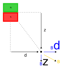
The magnet and the sensor (the dot), at axial distance \(z\) below the magnet's centre and radial distance \(d\) from its axis. The field at the sensor, \(B\), is the composition of its axial part \(B_z\), along the key's travel, and its radial part \(B_d\), pointing away from the axis.
Both parts are present at every position except on the axis (\(d = 0\), where \(B_d = 0\)) and level with the magnet (\(z = 0\), where \(B_d = 0\) and \(B_z = -K/d^3\)). Their combined strength is
A sensor reads one direction of this combined field, its sensitive axis, whatever the sensor's technology. The angle \(\alpha\) is the direction of that sensitive axis, measured from the board plane (the radial direction, sideways) toward the magnet's axis (upward). The reading follows
The practical difference between TMR and Hall-effect (HE) sensors is that TMR sensors measure the field sideways, in the plane of the sensor (\(\alpha = 0\)), while HE sensors measure it through their face, upward (\(\alpha = 90°\)). This decides where each one goes. An HE sensor sits under the magnet, on its axis, where the field points straight up and down and is strongest. A TMR sensor cannot sit there: on the axis the field has no sideways part (\(B_d = 0\)), so a TMR sensor under the magnet would ideally read zero at every depth. It has to be mounted off the axis, beside the magnet, where the field lines bend sideways and \(B_d\) is not zero. Also, off the axis the reading no longer follows a simple power of the distance, so a TMR board needs its own travel curve (below).
While the formula is general and holds for a sensitive axis at any angle, for the two usual sensors, though, \(\alpha\) is either \(90°\) or \(0\), so one of the two terms vanishes: an HE sensor essentially measures \(B_z\), and a TMR sensor essentially measures \(B_d\).
- Hall-effect sensor under the magnet: \(\alpha = 90°\). It is sensitive through its face, so it measures the field in the upward direction, and centred on the axis (\(d = 0\)) the field there is purely axial: the reading is \(B_z\) alone.
-
TMR sensor beside the magnet: \(\alpha = 0\). It measures the radial part \(B_d\). The field at its position is not purely radial. It is a composition of the axial and radial parts, and their proportion changes along the keystroke as \(z\) shrinks. With its sensitive axis pointing at the magnet's axis, it reads \(B_d\), and turning that axis by an angle \(\varphi\) within the board plane scales the reading by \(\cos\varphi\). But any tilt of the sensitive axis out of the board plane (from the package, its mounting or its datasheet's axis definition) mixes \(B_z\) into the reading through \(B_\mathrm{sensor}\) above, and the axial part has a different shape, with its own peak and a sign change. Model the reading with \(B_\mathrm{sensor}\), not with \(B_d\) alone, unless the sensitive axis is known to lie in the board plane.
-
What
MAG_CURVE_POWERassumes. The power curve (step 3) replaces these expressions by their asymptotic form for a large distance. Far from the magnet (\(z \gg d\)), the axial part tends to \(B_z \approx 2K/z^3\) and the radial part, \(B_d \approx 3Kd/z^4\), dies out faster; on the axis (\(d = 0\)) the axial part alone remains even up close. What is left is a single power of the distance, \(\lvert B \rvert = K'/z^n\), with \(n = 3\) for the dipole, the library default. The curve keeps that form but leaves the exponent \(n\) as a parameter, because close to the sensor a real switch magnet is not a point and its field departs from the dipole's \(1/z^3\). A sensor meant to use this curve should be centred under the magnet: an offset brings back the radial part and changes the shape of the curve (next bullet). - What the measurements show. The depth sweep of the Praxis HE, sensor on the axis (Result on the Praxis HE, below), confirms that the power-law approximation is valid for this key: with a fitted exponent, \(n = 1\), the curve predicts the key's depth within 0.08 mm rms (0.21 mm at worst) on the way up, against 0.97 mm rms for no curve at all. It does not confirm the dipole's own exponent: with \(n = 3\) the error is 0.35 mm rms. The approximation therefore holds as a power law with a fitted exponent, not as the far-field dipole itself. This is one sweep of one key, and the exponent cannot be separated from the zero field there: \(n \approx 2.4\) with a zero field of about 2164 fits as well as \(n = 1\) with 2048. More keys and a measured zero field will tell which applies.
- Off the axis (\(d > 0\)), neither component is a power law of \(z\). Far away (\(z \gg d\)) they tend to \(B_z \approx 2K/z^3\) and \(B_d \approx 3Kd/z^4\); closer in, both rise to a peak and fall again, and so does a reading that combines them, its peak moving from \(B_z\)'s to \(B_d\)'s as \(\alpha\) goes from 90° to 0 (at \(\alpha = 45°\), \(z \approx 0.77\,d\)). \(B_z\) peaks at \(z = \sqrt{3/2}\,d \approx 1.22\,d\), crosses zero at \(z = d/\sqrt{2} \approx 0.71\,d\) and reverses below that; \(B_d\) peaks at \(z = d/2\) and is zero when the magnet is level with the sensor (\(z = 0\)).
A travel curve needs a reading that is monotonic in travel, so off the axis the whole keystroke must stay on one side of the peak, with some margin: the curve flattens toward the peak, and resolution with it. Rest and bottom readings alone cannot show which side a key is on, so the geometry (\(d\), \(z_\mathrm{rest}\), \(\alpha\) and the travel length) has to guarantee it; check it when placing the sensor in step 2. Neither expression can be solved for \(z\) in closed form: a curve for such a geometry inverts it numerically into a lookup table, or uses a table of reading against depth measured with the sweep below (Fitting other curves). These are dipole expressions, so near the magnet they carry the same error as on the axis; fit their parameters (\(K\), \(z_\mathrm{rest}\), \(d\), \(\alpha\) and the zero field) to a sweep rather than taking them from the magnet's datasheet. How to add such a curve to MAGDA: MAGDA architecture, section 3.2.
What you need
- A caliper or dial indicator in a fixture that pushes one keycap straight down and holds it at a set depth, both hands free.
- A key that is easy to reach and has no stabilizer (a 1u key near the board's edge): on long keys, a caliper away from the switch measures keycap tilt, not switch travel.
- The firmware with
MAG_DUMP(console enabled), a calibration done, and the key's total travel from the switch datasheet (Praxis: 4.0 mm).
Measuring well
Most of the error in a sweep comes from the mechanics, not from the sensor. These hints address the faults seen in the Praxis dataset (see Limits of this dataset below):
- Push the stem, not the keycap. Remove the keycap and press the switch stem itself with a flat tip, straight down along its axis; zero the gauge on the stem with the key at rest. A keycap tilts and flexes, and on long keys it tilts around the stabilizer.
- Use a rigid, repeatable positioner. A dial indicator or a caliper's depth rod on a stiff stand is better than a hand-held caliper; a micrometer stage, a drill-press stand or a machine axis that moves in known steps (for example a 3D printer's Z axis driven by commands) removes most of the setting error. Check the positioner's own resolution (a dial indicator reads 0.01 mm).
- Keep magnetic material away. A steel caliper jaw or screwdriver next to the switch magnet changes the field the sensor sees. Use a non-magnetic tip (plastic, brass or aluminium) where it touches the stem, and keep other magnets and tools away from the board.
- Approach each depth from the same direction. Play and friction make a depth reached from above read differently from the same depth reached from below. Measure the way down and the way up as separate sweeps and compare them, or approach every depth from the same side (overshoot slightly and come back).
- Check the zero before and after. Read the rest level before starting and again at the end; a difference shows settling or drift during the run.
- Include the real bottom-out. Finish the stroke at the switch's hard stop and compare that reading with the key's calibrated bottom. Calibrate the key just before the sweep, pressing it the same way.
- Take smaller steps where it matters. The top of the stroke decides low actuation points and changes the reading least: measure in finer steps (for example
--plan 0:4:0.1: 81 depths down and back, about 13½ minutes). Keep one run per file:fit_marks.pytakes each file's shallowest depth as the key's rest and its deepest as the bottom. - Hold longer if readings creep. Increase
--holdand--useuntil the ± values stay small and the mean stops moving. - Measure the zero field. With a switch removed, log the bare sensor for a few seconds; that reading replaces the assumed half-supply value (2048) and removes the ambiguity between the exponent and the zero field.
- Repeat, and measure several keys. At least two sweeps per key, on keys with different rest levels (close to and far from the zero field); fit them together and look at the spread.
- Keep the conditions steady. Let the board run for a while before measuring, keep hands off the PCB, and note the room temperature; the sensor and the magnet both drift with temperature.
References: the switch's datasheet (total travel, pre-travel, force curve) for the depth range and the bottom-out; the sensor's datasheet (HAL4904: sensitivity, zero-field output, temperature coefficients) for the voltage and field estimates; python3 modules/acheron/mag/tools/pace_capture.py --help and fit_marks.py --help for every option.
Capturing
Two terminals. The first logs the keyboard's console to a file:
PYTHONUNBUFFERED=1 qmk console > sweep.log
MAG_DUMP must be streaming (check that raw lines appear in the log). It is a toggle: pressing it while it is already on switches it off.
The second runs the paced capture for the key being measured (matrix row and column):
python3 modules/acheron/mag/tools/pace_capture.py --key 0,7 --follow sweep.log --out sweep.csv
The script sets the pace so both hands can stay on the fixture: it shows MOVE to x mm (5 s, --move-time) and then HOLD (5 s, --hold), beeping at each change, and records the mean of the last 3 s of every hold (--use). The default plan goes from 0 to 4.0 mm in 0.25 mm steps and back up (--plan 0:4:0.25): 33 depths, about 5½ minutes. Each record is saved at once, so an interrupted run keeps what was done.
Analysing
python3 modules/acheron/mag/tools/fit_marks.py sweep.csv --n 1 --plot sweep.png
It splits the sweep into the way down and the way up, takes each direction's rest and bottom from its readings at 0 mm and at full depth, and prints the exponent that fits best and the depth error (rms and maximum, in mm) for n = 3, for --n and for the fitted value. A fit that lands at the edge of its search range means the power curve does not describe the key. The plot shows both directions with their fitted curves.
Fitting other curves
The sweep measures the key itself: a table of readings against physical depth, independent of any model. The same procedure therefore also fits the parameters of any other travel curve, for example one added for a different sensor type or placement (how to add a curve: MAGDA architecture, section 3.2). Capture the sweep in the same way, then choose the curve's parameters so that the travel it computes from each reading matches the measured depth (least squares over the points). fit_marks.py does this for the power curve's exponent; for another curve, its CSV (depth and mean reading per record) is the input for the same kind of fit.
Result on the Praxis HE
Top-left key (R0C7), caliper on the keycap above the stem, 0 → 4.0 → 0 mm in 0.25 mm steps:
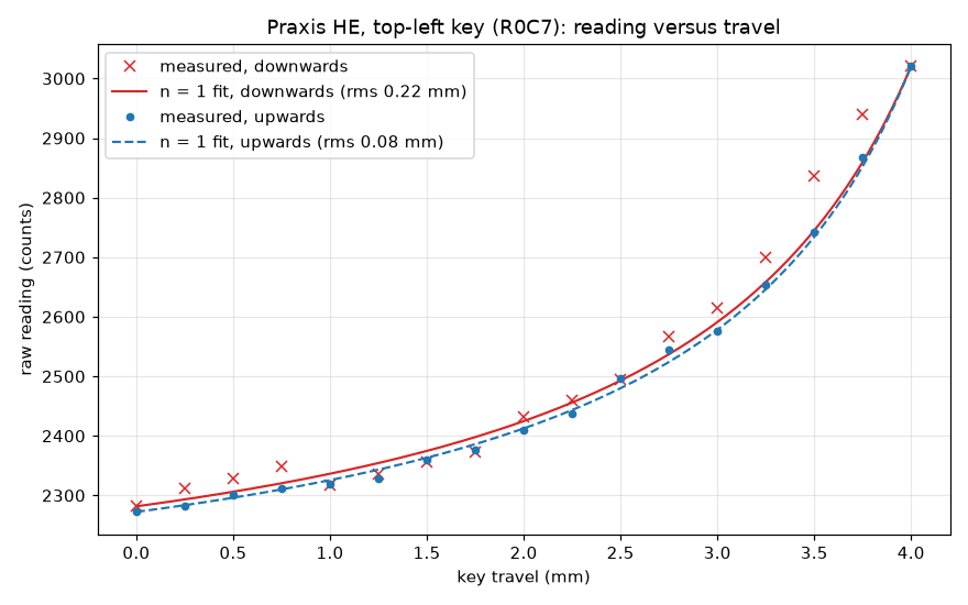
Red crosses: pressing down; blue dots: coming back up; lines: the power curve with n = 1 fitted to each direction.
The measured readings (raw counts; each the mean of 29–30 frames over the last 3 s of a 5 s hold; ± is the uncertainty of that mean). The 4.00 mm reading is the turning point, shared by both directions. The last two columns are estimates derived from the readings: the equivalent sensor output voltage, reading × 3.3 V ÷ 4096 (the ADC's reference is the 3.3 V rail; its actual voltage was not measured), and the magnetic field at the sensor, (reading − 2048) × 0.806 mV ÷ 1.4 mV/G, using the HAL4904's typical sensitivity and a zero-field output of half the supply (1 mT = 10 G). Both are only as accurate as those assumptions; in particular the zero-field reading is not measured (see the note on the exponent below).
| Travel (mm) | Reading, pressing down | Reading, coming back up | Equivalent voltage (V), down / up | Estimated field (mT), down / up |
|---|---|---|---|---|
| 0.00 | 2281.6 ± 1.3 | 2272.2 ± 1.0 | 1.838 / 1.831 | 13.4 / 12.9 |
| 0.25 | 2311.3 ± 1.3 | 2282.4 ± 1.1 | 1.862 / 1.839 | 15.2 / 13.5 |
| 0.50 | 2327.6 ± 1.1 | 2300.8 ± 0.9 | 1.875 / 1.854 | 16.1 / 14.5 |
| 0.75 | 2348.4 ± 1.1 | 2311.4 ± 1.1 | 1.892 / 1.862 | 17.3 / 15.2 |
| 1.00 | 2317.9 ± 1.1 | 2318.6 ± 1.2 | 1.867 / 1.868 | 15.5 / 15.6 |
| 1.25 | 2335.5 ± 1.0 | 2328.4 ± 1.3 | 1.882 / 1.876 | 16.5 / 16.1 |
| 1.50 | 2356.1 ± 1.1 | 2360.4 ± 1.2 | 1.898 / 1.902 | 17.7 / 18.0 |
| 1.75 | 2373.2 ± 0.9 | 2375.8 ± 1.2 | 1.912 / 1.914 | 18.7 / 18.9 |
| 2.00 | 2431.3 ± 1.5 | 2409.0 ± 1.2 | 1.959 / 1.941 | 22.1 / 20.8 |
| 2.25 | 2458.7 ± 1.2 | 2437.2 ± 1.0 | 1.981 / 1.964 | 23.6 / 22.4 |
| 2.50 | 2495.0 ± 1.4 | 2496.3 ± 1.2 | 2.010 / 2.011 | 25.7 / 25.8 |
| 2.75 | 2565.9 ± 1.1 | 2545.2 ± 1.1 | 2.067 / 2.051 | 29.8 / 28.6 |
| 3.00 | 2615.4 ± 1.3 | 2575.0 ± 1.1 | 2.107 / 2.075 | 32.7 / 30.3 |
| 3.25 | 2699.0 ± 1.4 | 2652.8 ± 2.1 | 2.174 / 2.137 | 37.5 / 34.8 |
| 3.50 | 2836.1 ± 2.0 | 2742.4 ± 1.4 | 2.285 / 2.209 | 45.4 / 40.0 |
| 3.75 | 2940.5 ± 1.9 | 2867.1 ± 3.6 | 2.369 / 2.310 | 51.4 / 47.1 |
| 4.00 | 3020.6 ± 1.4 | 3020.6 ± 1.4 | 2.434 / 2.434 | 56.0 / 56.0 |
Why measure raw readings, and not the voltage with a voltmeter
The raw readings are exactly what the firmware works with, so measuring them directly leaves nothing to assume or convert:
- No assumptions about the supply or the sensor. A voltage has to be converted to counts before it means anything to the firmware, and that needs the ADC's reference voltage and the sensor's zero-field output (assumed to be exactly half the supply). The raw reading already contains both: the sensor and the ADC share the 3.3 V rail, so the exact supply voltage cancels out.
- The ADC's real behaviour is included. Its actual gain, offset and linearity errors, its 12-bit resolution, and the settling through the multiplexer and the sample time are all part of the reading, as they are during normal use. A voltmeter measures the sensor pin before all of that.
- The same path as in use. The readings come through the same multiplexer, sample timing and scan as the firmware's own; a voltmeter probe at a sensor output would also load the node and average differently.
The voltage and field columns above are therefore estimates derived from the raw readings, for orientation; the fit uses the raw readings.
Limits of this dataset
Treat these numbers as a first measurement, not a characterisation of the Praxis HE (how to avoid these faults: Measuring well, above):
- One key, one sweep. Only the top-left key (R0C7) was measured, once. Whether other keys, with different rest levels and magnets, follow the same curve is not known yet, and the sweep was not repeated to check reproducibility.
- A slip on the way down. At 1.00 mm pressing down the reading (2317.9) is lower than at 0.75 mm (2348.4), which cannot happen for a key moving deeper; the fixture most likely slipped. This is one reason the fit relies on the way up.
- Down and up disagree. At the same caliper depth, pressing down reads higher than coming back up, by up to 94 counts (at 3.50 mm): friction and play between caliper, keycap and stem make the caliper depth differ from the switch's real position, differently in each direction.
- Rest moved during the run. The reading at 0 mm was 2281.6 at the start and 2272.2 at the end, 9 counts apart: settling of the key or the fixture, or drift.
- The deepest point is not the calibrated bottom. At 4.00 mm the reading was 3020.6, against a calibrated bottom of 3135: the caliper stroke did not reach the switch's full bottom-out (or calibration pressed harder). The fit uses the measured 4.00 mm reading as the bottom, while the firmware uses the calibrated one.
- Steps near the top are small. Near rest, 0.25 mm changes the reading by only 10–18 counts, so small fixture errors there weigh heavily on the fitted curve.
- The zero-field reading is assumed, not measured. The fit and the field column assume 2048; with this single key, n ≈ 2.4 with a zero field of about 2164 fits as well as n = 1 with 2048.
- Uncontrolled conditions. Temperature and the exact supply voltage were not recorded, and the ± values only cover noise, not these systematic errors.
| Curve (zero field 2048) | Way up: depth error | Way down: depth error |
|---|---|---|
| n = 3 (library default) | 0.35 mm rms, 0.52 mm max | 0.35 mm rms, 0.65 mm max |
| n = 1 | 0.08 mm rms, 0.21 mm max | 0.22 mm rms, 0.42 mm max |
| linear (no curve) | 0.97 mm rms, 1.38 mm max |
- With n = 3, keys actuated deeper than set on this key: 60 % at about 2.84 mm instead of 2.40 mm, 10 % at 0.58 mm instead of 0.40 mm. The Praxis HE therefore ships with
MAG_FIELD_EXPONENT1.0. - The way up fits better than the way down: pressing down, the reading runs slightly ahead of the caliper (friction and play between caliper, keycap and stem), so the way up is the cleaner curve.
- One key cannot separate the exponent from the zero-field reading: n ≈ 2.4 with a zero field of about 2164 fits this key as well as n = 1 with 2048. Measuring a bare sensor (a switch removed) settles the zero field; more keys with different rest levels show whether one exponent suits the whole board.
- A more accurate curve moves low actuation levels to where they belong, which is closer to rest in raw counts: on the Praxis calibration, at 10 % the gap between press and release shrinks from 7–17 counts (n = 3) to 3–11 counts (n = 1). Repeat step 10's tests at low levels after changing the exponent.
Possible problems
- Missing or doubled depths. Near the top of the stroke a 0.25 mm step changes the reading by only 10–20 counts, less than the raw noise; a tool that looks for steady readings cannot see those steps. The paced capture avoids this by recording on a fixed schedule instead.
- Readings creeping during a hold. The keycap or the fixture settles after each move. Averaging only the last seconds of the hold, and a stiff fixture, help.
- The deepest reading far from the calibrated bottom. The caliper is not measuring the switch's travel (tilt, flex, a caliper not above the stem), or the key was pressed harder during calibration. On the Praxis HE, 4.0 mm reached 3021 counts against a calibrated bottom of 3135.
- The key sends keystrokes while measured. Each pass through the actuation point sends the key's keycode (on the Praxis HE's top-left key, Win). Choose a harmless key, or remap it temporarily.
- No data in the log.
MAG_DUMPswitched off by pressing it while it was already on; orqmk consoleoutput held back when redirected (usePYTHONUNBUFFERED=1). The capture script warns when no frames arrive.
Setting the value
Put the result in the board's config.h as MAG_FIELD_EXPONENT (a float, e.g. 1.0f); every unit ships with it. Users can override it through a configurator app where the board supports one (e.g. a Field exponent slider in VIA, × 10); EE_CLR returns to the factory value. Changing the exponent changes the margins: repeat step 10.
Step 12: Factory calibration table (optional)
A factory table is worth having because it makes the PCBs pre-calibrated: a board works properly the moment it is assembled and flashed, with no calibration step for the user, and it falls back to a sensible state after EE_CLR instead of to provisional keys. This is most useful when the switches the board will be used with are known in advance, as on a keyboard sold with a specific switch: the table is taken with those switches, and every unit starts close to right. With a different switch (another magnet, strength or pole) the table no longer fits, and users have to calibrate their own.
Still, in most use cases users will need to calibrate their build again, because of variations in switch, sensor and PCB manufacturing, so the factory settings will most likely only be useful for preliminary testing.
Calibrate one unit carefully (every key fully, long keys in the centre), check the spans (step 8), and paste the mag_default_cal table printed by MAG_CAL_DUMP into the board's source. Every board flashed with the firmware then works calibrated from the start and after EE_CLR; users still calibrate their own for the best result. How: driver documentation.
Pass: after EE_CLR, with no calibration, keys work normally at the default actuation level (MAG_CAL_DUMP shows (factory) for every key).
Step 13: Configurator support (optional)
MAGDA exposes its settings and keycodes through QMK's VIA protocol, so a configurator app such as VIA can show them as sliders, switches and custom keycodes. Offering this is the board's choice. For VIA: add the forwarding, a via keymap and a VIA JSON with the Magnetic switches menu and the MAGDA custom keycodes (driver documentation). On MCUs with few USB endpoints (STM32F411), VIA with the console needs KEYBOARD_SHARED_EP = yes.
Test by loading the JSON in VIA's Design tab: the board opens, the sliders and switches change the settings (the console confirms each change), and saving works. A build without VIA is detected by VIA but cannot be opened. VIA's saved keymap persists on the keyboard; it is reset by EE_CLR, or when a VIA build from a different day is flashed.
Step 14: Release
- Remove temporary bring-up code (e.g. streaming at power-up, test timing overrides).
- Run
qmk lint -kb <keyboard>and fix what it reports. QMK keeps VIA keymaps and VIA JSON files out of its repository: keep them out of an upstream submission. - Write the board's
readme.md: build and flash commands, bootloader entry, whereMAG_CAL,EE_CLRand the other MAGDA keycodes sit, the indicators, and a link to Magnetic Switches. - Record your measurements (noise, timing, spans, the tuning results) with the board: they are the reference when a unit misbehaves later.
Reference Design: Praxis HE
The Praxis HE is the reference design for MAGDA: a 66-key angled keyboard with linear Hall sensors, five analog multiplexers and an STM32F411, running the stock mux_adc driver. This part describes its hardware and its port onto MAGDA, as a complete, working example to copy from. The steps above refer to it throughout; the firmware is in keyboards/aeboards/praxis_he/.
The board's development record (bring-up phases, every hardware measurement and anomaly, open issues) is kept with the PCB sources, in ARCHITECTURE.md of the Praxis HE PCB repository; this part calls it the board record.
1. Hardware summary
1.1 Sensing chain
- 66 linear Hall sensors (
HAL4904, SOT-23, VCC/OUT/GND), one centered under each magnetic switch. - 5 × CD74HC4067 16:1 analog muxes, one per electrical row.
- Mux r COM → MCU ADC input for row r; mux input c ↔ column c.
- All five muxes share the select lines and the enable, so one select value exposes one column across all five rows simultaneously.
- Sensor supply is
+3V3, which is also VDDA/VREF+. Readings are therefore ratiometric: supply drift cancels to first order. - No hardware power gating for the sensors. They draw current whenever the board is powered.
1.2 MCU and pin map
MCU: STM32F411CEU6. Bootloader: ST ROM DFU (stm32-dfu).
| Function | Pin | Notes |
|---|---|---|
| ROW0_MUX … ROW4_MUX | PA0 … PA4 | ADC1_IN0 … ADC1_IN4 |
| MUXSEL_S0 (LSB) | PB14 | shared by all muxes |
| MUXSEL_S1 | PB13 | |
| MUXSEL_S2 | PB10 | |
| MUXSEL_S3 (MSB) | PB1 | |
| MUXEN | PB12 | 4067 ~E, active low, all muxes |
| RGB data | PB15 | → TXS0101 (3.3 → 5 V) → SK6812MINI-E ×3, chain D2 → D3 → D4 |
| Flash SCK / MISO / MOSI | PA5 / PA6 / PA7 | SPI1, W25Q128JV (16 MB NOR) |
| Flash CS | PB0 | |
| USB D− / D+ | PA11 / PA12 | full-speed; PA9 is not wired to VBUS |
| SWDIO / SWCLK | PA13 / PA14 | header X1 |
| BOOT1 | PB2 | 10 k pull-down |
| HSE | PH0 / PH1 | Y1 7325-0800A2010-00, 8 MHz |
| Spare GPIO | PA8, PA9, PA10 (X2); PA15, PB3–PB9 (X3); PC13–PC15 (X4) | unused by default |
Bootloader entry is hardware: tap the reset button to reset, hold it about 2 s or more to enter DFU. Firmware needs no special handling beyond QK_BOOT.
1.3 Electrical matrix
5 rows × 15 columns used (mux inputs I0–I14). Input I15 is tied to GND on every mux.
Populated positions (66):
| Row | Columns present |
|---|---|
| 0 | 0–14 |
| 1 | 0–14 |
| 2 | 0–14 |
| 3 | 1–14 |
| 4 | 3, 4, 5, 6, 8, 10, 14 |
Unpopulated mux inputs are tied to GND: R3C0, R4C0, R4C1, R4C2, R4C7, R4C9, R4C11, R4C12, R4C13, and I15 on all rows.
The mapping from electrical position to physical key and keycap label must be derived from the sources:
- Physical position: the PCB file matches each sensor (net
RrCc) to its switch footprint's position, rotation and size. - Default keycode: the text labels next to the sensors in
sensors.kicad_sch.
The layout is angled (rotated switches), with split backspace, split spacebar and two MO1 keys.
Derivation results (used for keyboard.json and the default keymap):
- Every sensor sits exactly at its switch footprint's centre. Switch footprints are
acheron_MXHE:MX<size>HE(1u to 2.75u), all onF.Cu. - The PCB coordinates are mirrored in x relative to the key labels (ESC, CAPS, LCTL at the largest x). The layout is drawn mirrored in x, so ESC is top-left. Switch rotations of ±12° map to QMK
r= ±12 (left block +12, right block −12); footprints rotated 180° or ±168° only flip stabilizer orientation. - Label interpretation:
SLSHat R1C7 (1.5u, end of the Q row) is backslash;SLSHat R3C7 is slash.PLUSis the=/+key (KC_EQL). Split backspace:LBSPC(R0C8) =KC_BSPC,RBSPC(R2C8) =KC_DELby the labels; the default keymap putsKC_BSLSonLBSPCandKC_BSPCon the backslash key instead (section 2.5).Bappears on both halves. - By geometry, the left
MO1(R4C3, 1.25u) sits to the right of the left space bar (R4C4, 2u).
1.4 Hardware facts that affect firmware
- Mux settling. Each
ROWn_MUXtrace is 190–240 mm long. Firmware must wait after changing S0..S3 before sampling, and use an adequate ADC sample time. - Sensor supply voltage. Resistive drop on
+3V3is 0.4–3.8 mV per mA of per-sensor current, so 0.6–5.3 mV at the sensors' 1.4 mA. This is a small static per-key offset and gain difference, absorbed by per-key calibration. - USB suspend current. The ungated sensors draw about 92 mA, far above the USB suspend limit of 2.5 mA. Firmware cannot fix this; do not spend effort on it.
- Polarity and rest level are learned. The switch magnet biases the sensor even with the key released, so rest is not at mid-scale, and press direction depends on magnet orientation. Firmware stays polarity-agnostic and learns rest and bottom-out per key.
1.5 Sensor characteristics (HAL4904)
From the manufacturer's data, at 3.3 V. ADC counts assume the 12-bit ADC, 1 count ≈ 0.81 mV.
| Parameter | Value | In ADC terms / consequence |
|---|---|---|
| Supply current | 1.4 mA typical | 66 sensors ≈ 92 mA on +3V3 |
| Output at zero field | VDD/2 (not specified further); used as MAG_ZERO_FIELD (library default 2048) by the travel curve |
≈ 2048 counts for the bare sensor |
| Sensitivity | 1.4 mV/G | ≈ 1.7 counts/G; linear range ≈ ±1180 G from mid-scale |
| Output range | 0 to VDD, slightly nonlinear near the rails | rail check for invalid keys sits a little inside 0 and 4095 |
| Output noise | 1.4 mV RMS | ≈ 1.7 counts RMS, ≈ 12 counts peak-to-peak; ≈ 0.2 counts on a 64-frame rest average |
| Response time | ≈ 1 µs (power-up time 4 µs) | never limits scanning |
| Output resistance | 120 Ω | with mux on-resistance, settling well under 1 µs |
| Polarity | S pole at marked face lowers output (sense reversed in SOT-23) | direction learned per key |
The rest-to-bottom span depends on the switch magnet and is known only after calibration.
2. Port onto MAGDA
The analog machinery comes from the MAGDA community module acheron/mag (MAGDA architecture), enabled in keyboard.json. This board provides only configuration, the key mask and its peripherals.
2.1 Backend
The board uses the stock mux_adc driver. The sensing chain matches it exactly: muxes per row, shared select lines and enable, identity input mapping.
| MAGDA macro | Value |
|---|---|
MAG_MUX_SEL_PINS |
{ B14, B13, B10, B1 } |
MAG_MUX_EN_PIN |
B12, with MAG_MUX_EN_ACTIVE_LOW |
MAG_MUX_ADC_PINS |
{ A0, A1, A2, A3, A4 } |
MAG_MUX_PER_ROW |
defined |
MAG_SETTLE_US, MAG_ADC_SAMPLE_TIME |
2 and ADC_SAMPLE_28 (phase 3: no carryover down to 0 / ADC_SAMPLE_15; two steps of margin on both). #ifndef-guarded in config.h so test builds can override them via EXTRAFLAGS. Phase 2 used 5 / ADC_SAMPLE_56 |
Matrix: 5 × 15 (I15 is not part of the matrix).
mag_key_mask follows from section 1.3:
const matrix_row_t mag_key_mask[5] = {
    0x7FFF,   // row 0: cols 0-14
    0x7FFF,   // row 1: cols 0-14
    0x7FFF,   // row 2: cols 0-14
    0x7FFE,   // row 3: cols 1-14
    0x4578,   // row 4: cols 3,4,5,6,8,10,14
};
Self-test. Board override of mag_hw_selftest(): read I15 on all rows and check that it is near 0. This needs one extra select step, so run it at boot and occasionally, not on every scan. It needs either a driver helper or a board-side read; decide when implementing. Not implemented (open issue in the board record, section 5): the library never calls mag_hw_selftest(), and what to do on failure is undecided (MAGDA architecture, section 2).
Estimated timing. With about 1 µs of settling and 6–10 µs for the five conversions, a column takes about 7–11 µs and a full scan about 0.1–0.2 ms.
At the phase 2 starting values: the ADC clock is 24 MHz (96 MHz APB2, ADC_CCR_ADCPRE_DIV4), so one 12-bit conversion at ADC_SAMPLE_56 takes 68 cycles ≈ 2.8 µs, a column ≈ 5 + 5 × 2.8 ≈ 19 µs, and a full scan ≈ 0.3 ms plus adcConvert call overhead. Measured at the final timing: about 2000 main-loop passes per second (the board record, section 4.2).
2.2 Storage
Calibration and settings use the MAGDA datablock.
Backing store: QMK wear-leveling on the external W25Q128 (16 MB NOR) over SPI1. It is selected in keyboard.json, so MAGDA does not depend on it:
"eeprom": {
    "driver": "wear_leveling",
    "wear_leveling": {
        "driver": "spi_flash",
        "backing_size": 65536,
        "logical_size": 4096
    }
}
logical_size. Wear-leveling keeps a RAM copy of the logical EEPROM. The driver's default is 32 KB, a quarter of the F411's RAM, so it is set to 4096 bytes. That covers QMK's settings, the MAGDA datablock (under 1 kB) and a VIA keymap.backing_size. One 64 KB erase block of the W25Q128. It must be a multiple oflogical_size.
Flash and SPI configuration in config.h:
| Define | Value |
|---|---|
EXTERNAL_FLASH_SPI_SLAVE_SELECT_PIN |
B0 |
EXTERNAL_FLASH_SIZE |
(16 * 1024 * 1024) |
SPI_DRIVER |
SPID1 |
SPI_SCK_PIN / SPI_MISO_PIN / SPI_MOSI_PIN |
A5 / A6 / A7 |
QMK's defaults for page size (256 B), sector size (4 KB), block size (64 KB) and 3-byte addressing already match the W25Q128.
2.3 DMA streams
The sensor ADC, the flash SPI and the LED PWM each use DMA, and on STM32F4 no two peripherals may share a DMA stream: a stream serves one transfer at a time, and ChibiOS allocates each stream to one driver. Stream (and channel) choices are fixed by the reference manual's DMA request tables, so check them when picking pins and peripherals, not only after.
| Peripheral | Use | DMA stream | Source |
|---|---|---|---|
| ADC1 | sensor rows (mux_adc) |
DMA2 stream 4 | generic F411 mcuconf.h |
| SPI1 RX / TX | external flash | DMA2 streams 0 / 3 | generic F411 mcuconf.h |
| TIM1_UP | WS2812 PWM (PB15 = TIM1_CH3N) | DMA2 stream 5, channel 6 | board config.h |
All distinct. (SPI2, used for the LEDs before the PWM driver, would have used DMA1 streams 3/4.)
2.4 Board-specific peripherals
- RGB. 3 SK6812MINI-E used as indicators,
WS2812_DRIVER = pwmon TIM1: PB15 = TIM1_CH3N (AF1,WS2812_PWM_COMPLEMENTARY_OUTPUT), TIM1_UP DMA = DMA2 stream 5 channel 6 (ADC1 uses DMA2 stream 4). Same configuration askeyboards/smithrune/iron165r2/f411, an F411 board driving WS2812 from B15. Driven directly through QMK'sws2812API (WS2812_DRIVER_REQUIRED), no RGB Light. Assignment, 50% brightness (128), off otherwise: D2 Caps Lock (white); D3 the highest active layer (layer_state_set_kb,get_highest_layer): layer 1 white, layer 2 green (0,128,0); D4 rapid trigger (white;mag_rapidtrigger_kb(), also called at start-up with the stored state). Calibration mode: all three white. D3 as a layer indicator relies on the PWM driver's safe repeated flushes: the MO1 freeze with the SPI driver happened with layer-driven LED updates (the board record, section 4.7).mag_calibration_mode_kb()sets all three to 50% white while calibration runs. The PWM driver streams a circular DMA buffer andws2812_flush()only rewrites it, so repeated flushes are safe (why not the SPI driver: the board record, section 4.7). Verified on hardware. - USB. Full-speed, VID
0x4145, PID0x5048. VBUS sensing must be disabled, since PA9 is not connected to VBUS;GENERIC_STM32_F411XEalready setsBOARD_OTG_NOVBUSSENS, so no board override is needed. - Clock. QMK defaults
STM32F411toGENERIC_STM32_F411XE(platforms/chibios/mcu_selection.mk), which uses an 8 MHz HSE crystal. No"board"key, clock or PLL override.
2.5 Files
keyboards/aeboards/praxis_he/.
| File | Purpose |
|---|---|
keyboard.json |
MCU, bootloader (stm32-dfu), USB IDs, layout, matrix 5×15, debounce 0, EEPROM driver (2.2), custom matrix ("matrix_pins": {"custom_lite": true}), console ("features"), WS2812 PWM driver ("ws2812", 2.4), the MAGDA module ("modules": ["acheron/mag"]) |
post_rules.mk |
build settings keyboard.json cannot express: WS2812_DRIVER_REQUIRED = yes (LEDs driven directly through the ws2812 API, 2.4), MAG_DRIVER = mux_adc. The board has no rules.mk |
config.h |
MAG_* values from 2.1, flash and SPI config from 2.2, WS2812 config; board defaults MAG_ACTUATION_DEFAULT 614 (60 %) and MAG_RT_DOWN_DEFAULT / MAG_RT_UP_DEFAULT 102 (10 %); factory field exponent MAG_FIELD_EXPONENT 1.0f (the board record, section 4.9) |
halconf.h |
HAL_USE_PWM (LEDs), HAL_USE_SPI (flash). ADC needs no entry: the module's post_rules.mk sets ANALOG_DRIVER_REQUIRED, which defines HAL_USE_ADC (builddefs/common_features.mk) |
mcuconf.h |
enable ADC1 (sensor rows), SPI1 (flash) and TIM1 (LED PWM) |
praxis_he.c |
mag_key_mask, mag_default_cal (factory calibration from the phase 7 recalibration, the board record section 4.8), LED indication (led_update_kb Caps Lock, layer_state_set_kb layers, mag_calibration_mode_kb, mag_rapidtrigger_kb), and under VIA_ENABLE via_custom_value_command_kb forwarding to mag_via_command. No self-test override (2.1) |
readme.md |
end-user readme: calibrating, build and flash, VIA, bootloader entry, indicators, MAGDA keycode locations |
keymaps/via/keymap.c, keymaps/via/rules.mk |
VIA build: same layers as default; VIA_ENABLE, KEYBOARD_SHARED_EP. Git-ignored by QMK (.gitignore /keyboards/**/keymaps/via/*) |
via.json |
VIA definition: layout, Magnetic switches menu (actuation point, field exponent, rapid trigger switch and distance), custom keycodes (MAGDA architecture, section 4.5). Git-ignored by QMK (.gitignore via*.json) |
keymaps/default/keymap.c |
default keymap, derived as described in 1.3; layer 0: KC_LWIN on the top-left key (label ESC, R0C7), QK_GESC on the key left of 1 (label GRV, R0C6), left space bar (R4C4) is LT(2, KC_SPC) (tap: space, hold: layer 2); left half of the split backspace (R0C8) is KC_BSLS, right half (R2C8) KC_DEL, and the backslash key (R1C7) KC_BSPC, so Backspace sits in the Q row; layer 2: arrows on W/A/S/D (up/left/down/right), KC_HOME on PgUp, KC_END on PgDn, the rest transparent; layer 1: QK_BOOT (top-left key, R0C7), EE_CLR (Delete, R2C8; away from MAG_ACT_UP, the board record section 4.6), KC_NUM (A), KC_SCRL (S), MAG_DUMP (D), MAG_CAL (C), MAG_CAL_DUMP (V), MAG_ACT_UP (=, R0C9), MAG_ACT_DN (-, R0C10), MAG_RT_TOG (R, R1C1). Keymap grids (both keymaps) are wrapped in // clang-format off/on |